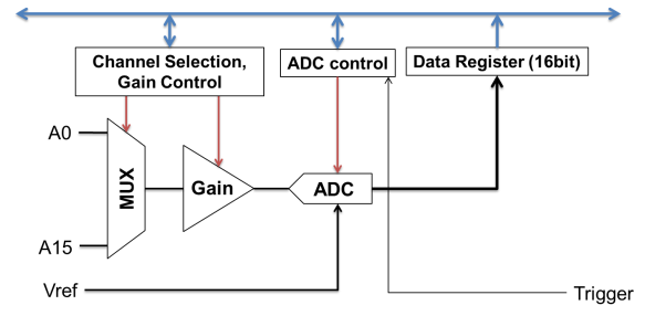
The AVR Atmega 2560 contains a single 10 bit analogue to digital converter (ADC) with a maximum sample rate of 15kS/s at full resolution. It uses a successive approximation type ADC. The AVR Atmega 2560 provides 16 analogue input pins that are selected using the MUX that is before the ADC. The input range is from 0-Vcc, where Vcc is typically 5V. Differential voltage measurements can also be made using four independent differential channels, or 14 channels referenced to two reference voltages. A simplified schematic of the ADC subsystems is shown in figure 1.
The ADC can be operated in the following three modes
- Single conversion: Started by writing a logical one to the ADC Start Conversion bit
- Triggered conversion: The conversion is initiated by the rising edge of the trigger input
- Free running:The next conversion takes place immediately after the previous conversion is finished
Before using the ADC it is necessary to select the reference voltage source and the ADC clock frequency. The voltage reference source options are shown in table 1 and are determined by setting bits 6,7 in the ADCMUX register shown in Figure 2.
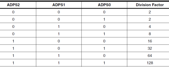
The ADC pre-scaler controls the internal ADC clock that controls the conversion process. By default, the successive approximation circuitry requires an input clock frequency between 50kHz and 200kHz. If a lower resolution than 10 bits is needed, the input clock frequency to the ADC can be as high as 1000kHz to get a higher sample rate. The conversion process requires 13-14 ADC clock cycles and this sets an upper limit on the sampling frequency. The pre-scaler options are shown in table 2.
When using a 16MHz oscillator then using a prescale value of 128 will give ADC clock frequency of 125kHz which is well within the 50kHz and 200kHz limits. It is also necessary to turn the ADC on and to ensure that the ADC is fully initialised carryout a single conversion by setting the ADSC bit in the ADCSRA register. Note this first conversion takes 25 clock cycles. The following function can be used to initialise the ADC for single conversion operation.
void adc_init(void){

//16MHz/128 = 125kHz the ADC reference clock

ADCSRA |= ((1<<ADPS2)|(1<<ADPS1)|(1<<ADPS0));

ADMUX |= (1<<REFS0);       //Set Voltage reference to Avcc (5v)

ADCSRA |= (1<<ADEN);       //Turn on ADC

ADCSRA |= (1<<ADSC); }     //Do an initial conversion
Once the ADC is initialised single conversions on any channel are carried out by first selecting the desired channel, starting the conversion and then polling the conversion complete flag (ADSC bit in the ADCSRA register, shown in figure 3) until the conversion is complete (ADSC=1 whilst the conversion is in progress and is set to ADSC=0 when the conversion is complete), then finally reading the converted value as shown in the UML activity chart of figure 5.
The following function can be used to acquire a single conversion from the specified single ended input channel
uint16_t read_adc(uint8_t channel){
ADMUX &= 0xE0;           //Clear bits MUX0-4
ADMUX |= channel&0x07;   //Defines the new ADC channel to be read by setting bits MUX0-2
ADCSRB = channel&(1<<3); //Set MUX5
ADCSRA |= (1<<ADSC);      //Starts a new conversion
while(ADCSRA & (1<<ADSC));  //Wait until the conversion is done
return ADCW;}         //Returns the ADC value of the chosen channel
This example allows you to select any of the 16 input channels that are available on the Atmega2560 for single ended voltage conversion, that is the voltage on the input pin is measured with respect the the microprocessor ground. The inputs can also be configured for differential voltage measurement by choosing the correct setting of the MUX bits. For more information look at table 26.4 in section 26.8.2 of the datasheet (pg. 290).


